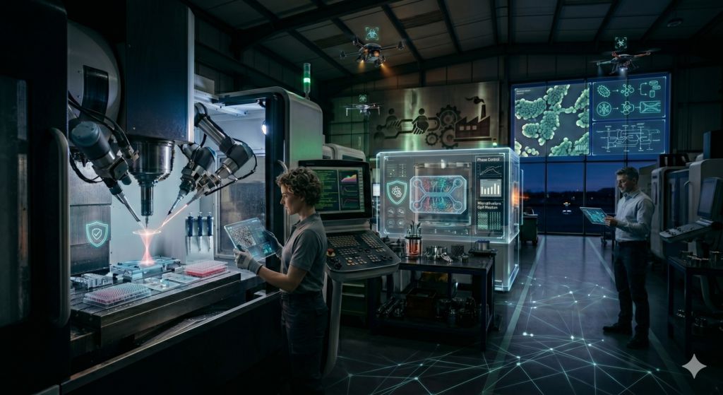
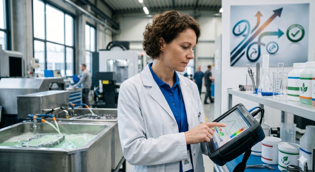
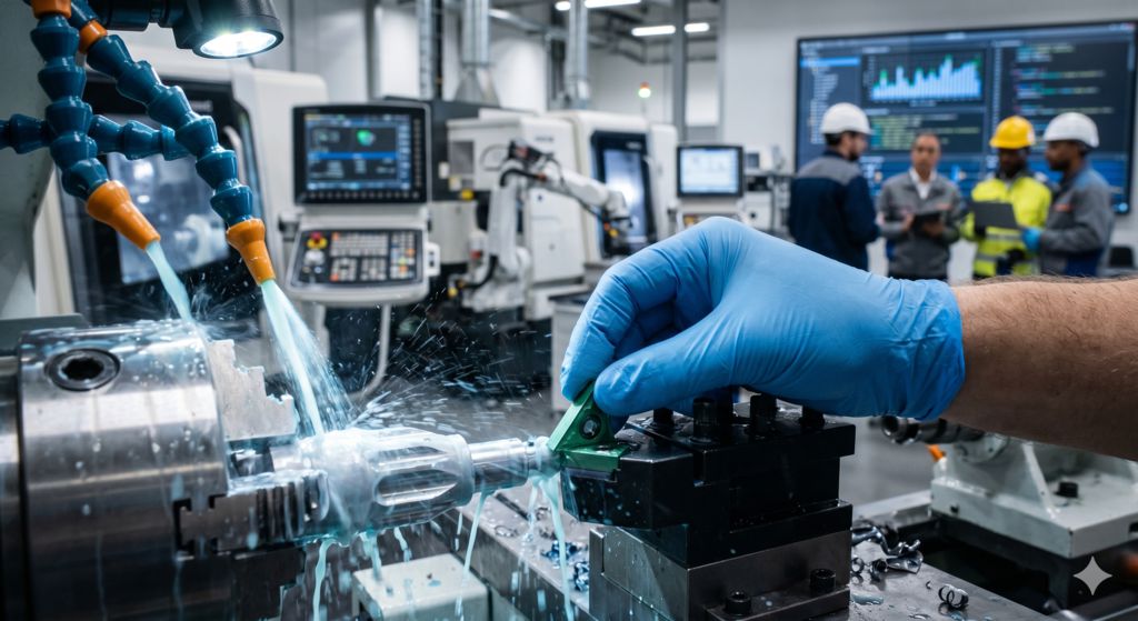
When we look at the history of manufacturing, our progress has always been defined by a single metric: scale. Thousands of years ago, humans shaped colossal stones with primitive hammers. Millennia later, we developed machines to mill steel to the precision of a millimeter. Today, advanced CNC machines and lasers routinely work within the realm of a micrometer—a fraction of the width of a human hair.
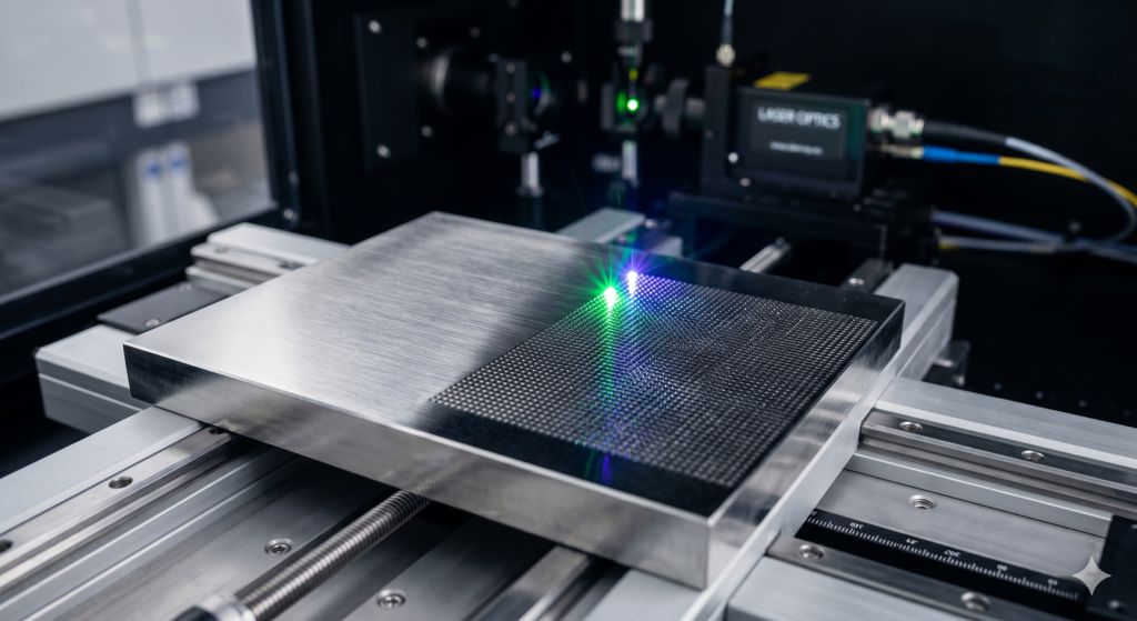
But as we push into the absolute frontiers of technology—powering artificial intelligence, advanced quantum computing, and next-generation medical sensors—even micrometers are too clumsy.
We have officially arrived at the era of Ultimate Manufacturing, where the new building block is the individual atom. At this extreme boundary, manufacturers no longer slash away blocks of metal or spray thick coatings. Instead, they rely on a breathtaking duo of chemical technologies: Atomic Layer Deposition (ALD) and Atomic Layer Etching (ALE).
By adding and removing materials exactly one atomic layer at a time, we are building a digital world with absolute molecular perfection. Here is how atomic-scale manufacturing works, and why it is transforming the future.
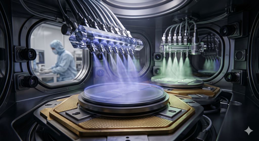
1. Atomic Layer Deposition (ALD): Building the Micro-Universe
Imagine you want to paint a complex, multi-layered sculpture so perfectly that the paint is exactly three atoms thick across every single crevice, curve, and hidden internal hollow. Spraying it would cause pooling; dipping it would create thick drips.
This is the exact challenge faced by microchip manufacturers. To solve it, they use ALD, a process that relies on self-limiting chemical reactions.
Instead of forcing a material onto a surface, ALD introduces gases called “precursors” into a sealed vacuum chamber in a highly controlled, four-step dance:
- First Precursor Pulse: The first gas fills the chamber. The molecules of this gas rush toward the workpiece and chemically bond with the surface. Crucially, once the surface is entirely covered by a single layer of these molecules, the reaction stops automatically. They cannot bond to each other.
- Purge: An inert gas (like nitrogen) blasts through the chamber, sweeping away any loose, unbonded precursor molecules.
- Second Precursor Pulse: A second gas is introduced. These molecules react aggressively with the first layer already stuck to the surface, transforming them into the desired final material—such as an ultra-pure oxide or metal film.
- Final Purge: The chamber is cleaned again, leaving behind a flawless, uniform coating exactly one atom thick.
By repeating this cycle hundreds of times, engineers can grow atomic structures layer by layer with absolute precision, ensuring identical thickness even inside microscopic holes that are thousands of times deeper than they are wide.
2. Atomic Layer Etching (ALE): The Atomic Scalpel
Building atom by atom is only half the battle. To create a functioning quantum computer or a hyper-dense microchip, you also need to carve away paths, channels, and gates. Traditional chemical etching or plasma blasting acts like an industrial sandblaster at this scale; it aggressively rips away material, damaging the surrounding atomic crystal lattice.
To achieve ultimate precision, engineers use the mirror image of ALD: Atomic Layer Etching (ALE).
Instead of aggressively dissolving material, ALE gently deconstructs it using a two-step atomic sequence:
- Modification: A specific gas (like chlorine) is introduced into the chamber. It reacts only with the outermost, exposed layer of atoms on the workpiece, chemically weakening their bonds to the rest of the material. The atoms directly beneath this top skin remain completely unaffected.
- Removal: The chamber is bombarded with a gentle pulse of low-energy ions or thermal energy. This targeted energy isn’t strong enough to damage the raw workpiece, but it is just energetic enough to knock off the weakened, modified top layer of atoms.
The result? The top skin of atoms vanishes completely, leaving behind a perfectly pristine, unmarred surface directly beneath it. By repeating this process, manufacturers can etch deep into a material atom-layer by atom-layer, achieving zero structural distortion and absolute edge control.
3. Why Atomic-Scale Control is Mandatory
Why go through the painstaking trouble of counting individual atoms during production? The reality is that humanity has hit a physical brick wall with traditional manufacturing.
As microchip components shrink down to just a few nanometers in size, they begin to experience a bizarre physics phenomenon called quantum tunneling.
If a protective insulating wall inside a chip is even one atom too thin, electrons will literally teleport right through the wall, causing a short circuit and rendering the processor useless.
ALD and ALE provide the absolute dimensional verification required to prevent these quantum leaks. They ensure that the atomic boundaries of tomorrow’s processors are perfectly uniform, allowing us to squeeze trillions of transistors onto a chip smaller than a fingernail without sacrificing thermal control or power efficiency.
4. Beyond Silicon: The Massive Future of Atomic Control
While the semiconductor industry is currently the primary driver of atomic layer processing, this technology is rapidly expanding into other high-stakes engineering sectors:
- Next-Generation Batteries: By coating battery electrodes with an ultra-thin ALD protective layer, engineers can prevent the internal chemical degradation that causes lithium-ion batteries to lose capacity over time, unlocking batteries that charge faster and last for decades.
- Advanced Medical Devices: ALD can apply biocompatible atomic coatings to micro-implants or neurological sensors, completely hiding the foreign metal or plastic from the human immune system and preventing implant rejection.
- Optical Masterpieces: Carving mirrors and lenses with ALE allows for the creation of flawless optical surfaces that can reflect or channel lasers with near-zero distortion, a critical requirement for deep-space telescopes and advanced laser weapons.
The Bottom Line
Manufacturing has officially transitioned from a mechanical science into a purely chemical, atomic art form. We are no longer merely shaping the materials that nature gave us; we are actively choreographing individual atoms to build custom matter from scratch.
Atomic Layer Deposition and Atomic Layer Etching represent the absolute pinnacle of human manufacturing precision. By mastering this atomic dance, we aren’t just pushing the boundaries of what machines can build—we are laying down the physical foundations for the next era of human technological evolution.
In addition, please visit CNC Turning Parts, Stamping Parts, Technical Data and Quality Inspection to get more information about us, if you have any question, please e-mail to Harry Yen hyen@unisontek.com.tw
Please watch our company YouTube channel Link and introduction Link